The Future of ASIC Cloud
Begins Here Beyond Imagination

Unfolding the ASIC Cloud Horizon

ASIC Accelerator Challenges and Innovations

Creative Needs for Massively Parallel Configuration and Innovation
Time to market Developing Processing Technology
Low-Power Carbon Emissions
Highly Efficient Low Voltage, Scalable Efficiency Design and Error-Free Technology Used to Implement Mass Commercialization for MPPA on a Chip
Substantial Layout Technique Requirements

Low noise
Fully differential
Ultra low power
Intricate matching scheme
Worldwide Deep Learning Chipset Sales
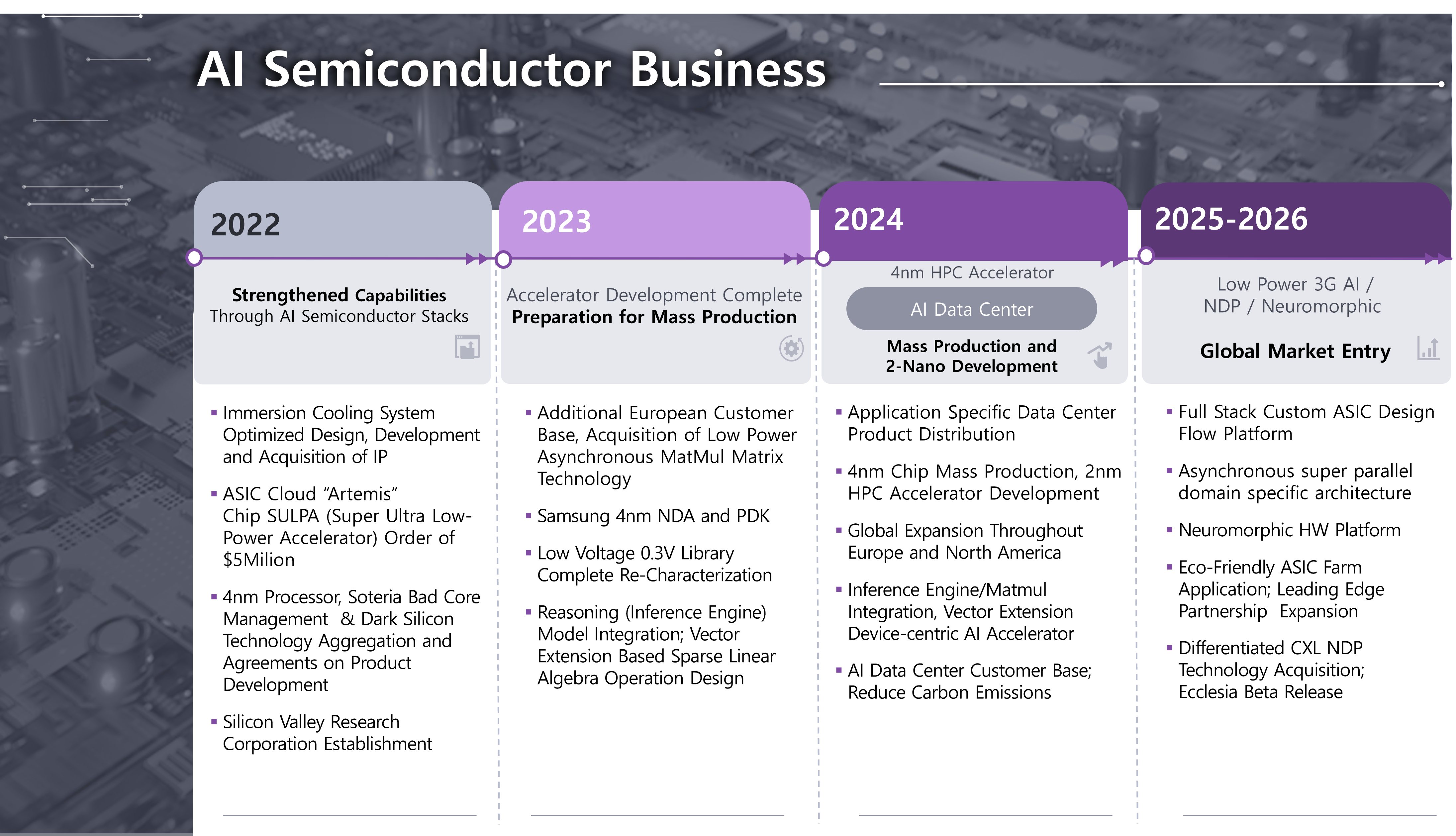
Hyper-Cloud Accelerator-Embedded ASIC Platform Roadmap
Our Breakthrough
ASIC Workload-Aware Reliable Design
Cross-layer holistic design optimization overcoming the limit of legacy development process
HPC ULPA ASIC : Ultra Low Power Structure
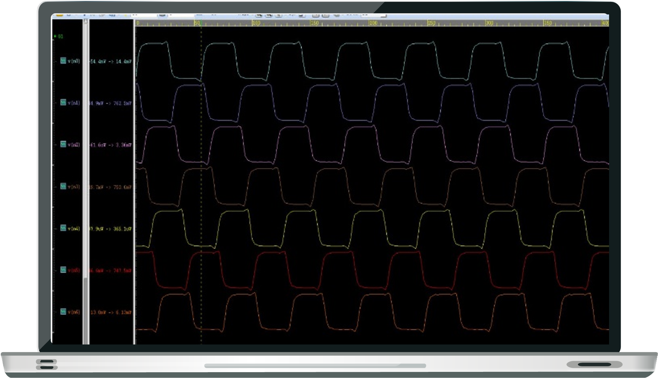
Near Threshold Voltage (NTV) Test Results

Soteria’s Various Models


• Ultra Low-voltage cells (Near-threshold cells)
• Special-purpose cells (Pulse-based, Multi-bit, Mixed-Vth)
• Layout-optimized cells (Multi-height PMK, Input sharing)
• Synthesis-friendly cells (Variable skews, Multi-setup/delay)
Unique Technological Prowess of Soteria
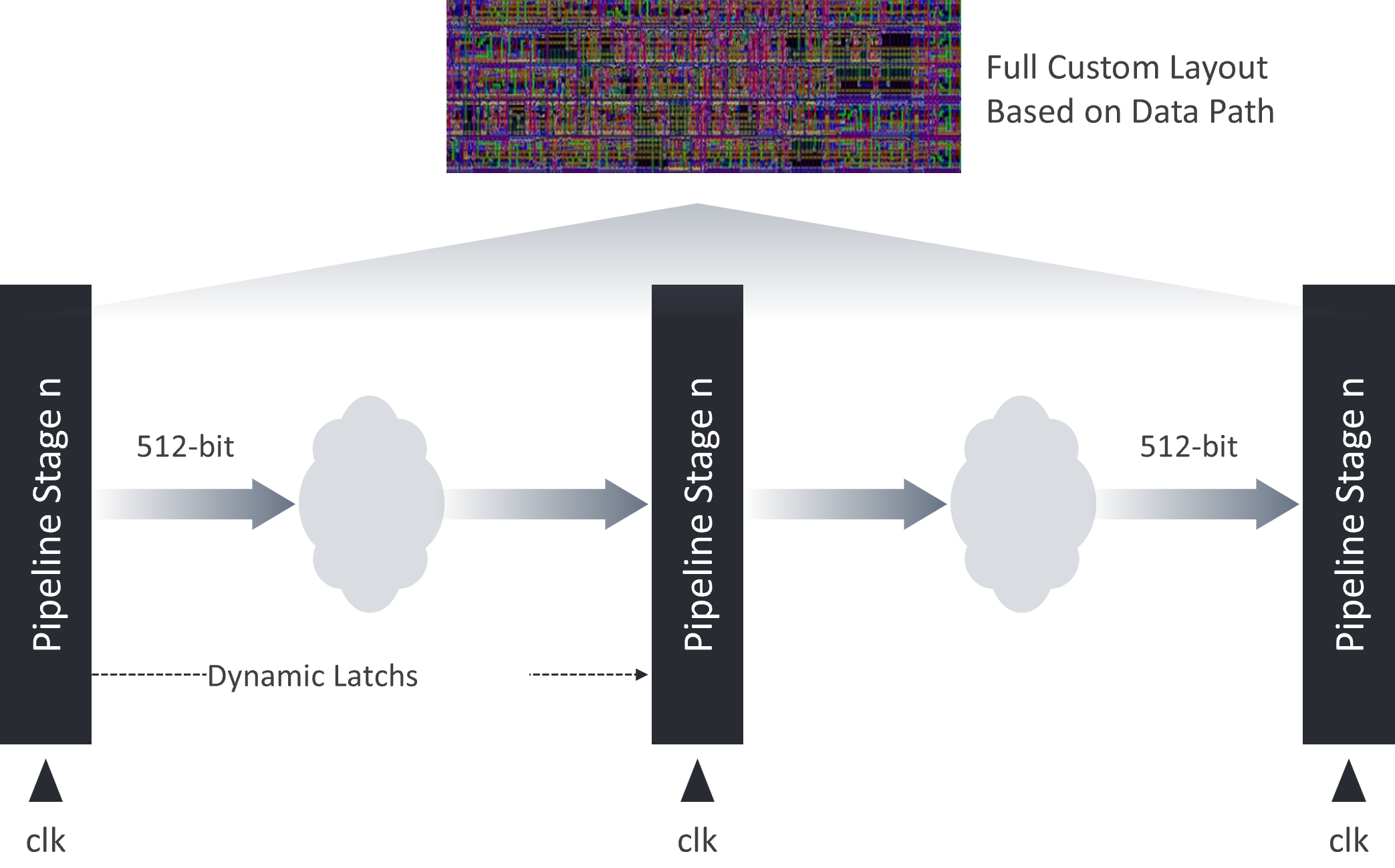
Computation Leveraging Dynamic Latch for Asynchronous Operations
 
Dynamic latches are state-of-the-art technology, specifically for asynchronous operations. Asynchronous operations refer to processes that run independently of each other without the need for synchronization to a common clock signal. This leads to a reduction in the time needed for synchronization between operations, thereby improving the overall efficiency of the system.
 
Leading innovation in asynchronous operations with several advantages such as faster processing times, efficient use of system resources, significant power savings.
Revolutionizing Energy Efficiency
Revolutionizing energy efficiency in data centers and orchestrating seamless operations for optimal performance

By providing an integrated system that considers both Immersion Cooling systems optimized for the data center environment and AI ASIC accelerators, efficiency and performance are maximized.
Interfacing with software equipped with management and monitoring functions, it supports the efficient operation of data centers.


The energy demand for data centers has exploded, consuming up to 5% of the world’s energy demand in 2025. Our company’s custom HPC accelerator, optimized for liquid cooling, is a future-leading technology that can solve this problem.

AI Accelerator Mass Production Technology

Amplifying the prowess of ultra-parallel HPC development, we’ve fine-tuned the architecture and design of AI ASIC accelerators, catapulting performance and energy efficiency to unparalleled heights.
Leveraging Workload Specific algorithms and cutting-edge optimization techniques, we’ve achieved a monumental leap in computational throughput.
We’ve engineered a dedicated hardware function for neural network acceleration, fortifying its integration or connectivity with existing System-on-Chips (SoCs)
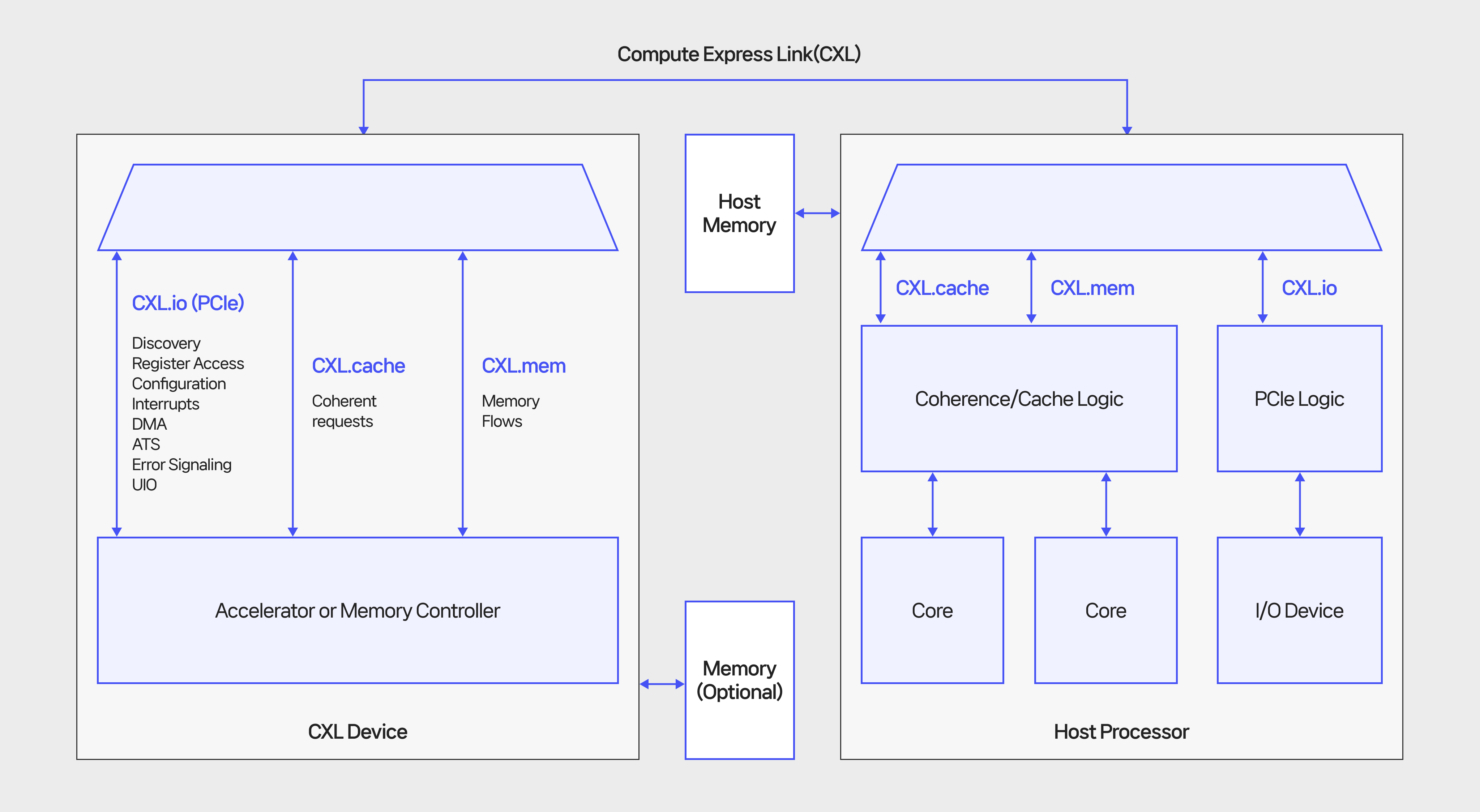
CXL Near Memory Computing Ecosystem NDP-CXL CHIP Architecture
Conceptual Diagram of Device Attached to Processor via CXL

Our system can reduce learning time in evaluation using various types of recommender system models compared to the latest system that connects large capacity new memory based on existing PCIe technology.
It helps improve computing performance by connecting accelerators, memory, and storage devices used with the CPU, and is a method of solving data processing delays, slowdowns, and scalability problems in existing systems.
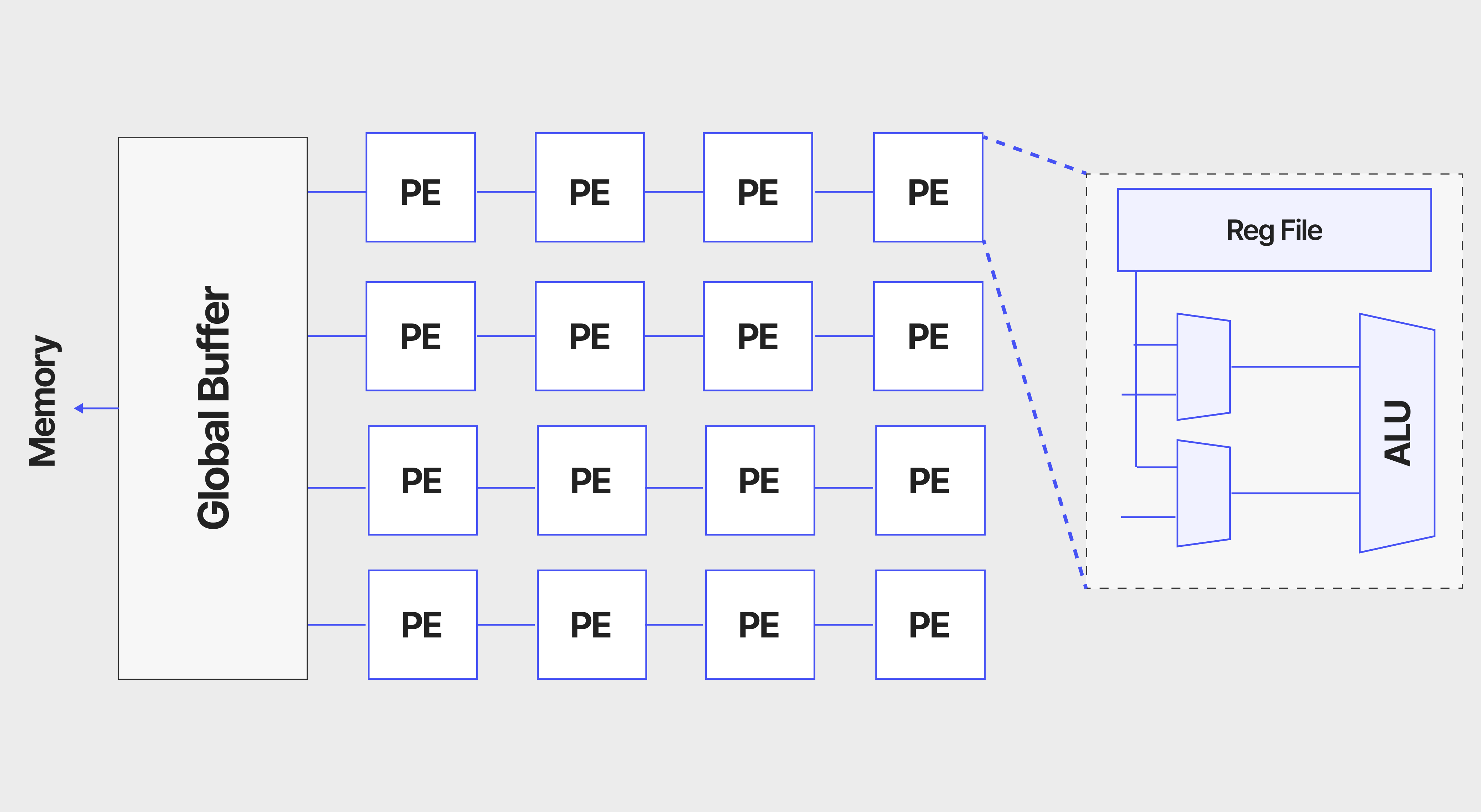
NDP-CXL CHIP

Architecture

Our system overcomes the limited performance limitations due to low bandwidth and memory capacity through CXL’s wide bandwidth and memory expansion capabilities.
By deploying an NDP module specialized for computation, data transmission overhead required during the computation process is reduced.
in Possession
Technology
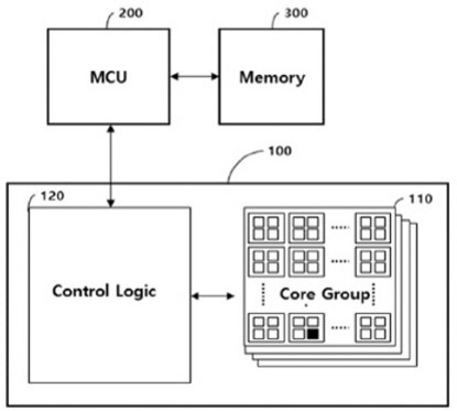
Multi-HW Accelerated Core Design Technology
Procurement of Multi-Core Motion Processing Technology for HW Accelerated Core Design and Maximized Parallel Performance
Bad Core Management Techniques
Bad Core Management System maximizes Dependability & Practicable Yield through detection and management of defective cores. This creative approach ensures optimal performance and reliability.
Multi-Chip Overcurrent Protection
Patent pending technology that prematurely prevents damage to operating chips due to overcurrent from defective chips.
Multi-Voltage Chip with IO Design
Specialized IO multi-voltage domain chips and specialized IO design technology ensure reliable and smooth data transfer.
Multi-Voltage Domain Chip Design Technology
More efficient chip operation is possible by using voltage appropriate for the function and area.
Full Custom Layout
Full custom layout technology is applied to increase thermal efficiency while using optimal area.While executing the chip layout, we connected the path supplying Power/Ground to each cell from the cell itself via the shortest path. This strategy ensures a heat dissipation path from the bottom cell to the top RDL, enabling rapid heat dissipation. Guided by Soteria & Samsung heat dissipation experts, this ingenious strategy not only enhances heat dissipation but also infuses a dash of innovation and efficiency into our technology, elevating it to a new immersion cooling system.
Revolutionized Low Voltage Behavior for Foundry Cell Technology
Advanced technology for development of a low power chip to overcome dark silicon Issue during development of multi-core parallel design. low voltage, high performance chip design re-characterized to operate at a lower voltage than regular foundry cell’s operating voltage.
Scroll to Top

Immersion Cooling is a highly efficient cooling solution that involves submerging servers in a non-conductive fluid.

Soteria’s Dependable Power Protection Circuit and Bad Core Management technology, along with firmware matching, are optimized for the maintenance of our client’s eco-friendly Data Center Immersion Liquid Cooling. This cooling method allows for direct contact between components and coolant, providing exceptional heat dissipation. Immersion cooling offers a myriad of benefits including improved cooling efficiency, reduced thermal stress, performance enhancement, extended equipment lifespan, and reduced physical installation space. Furthermore, immersion cooling eliminates the need for air cooling, allows for high-density placement, and reduces noise pollution in computing environments. This stunning, top-notch technology is the epitome of our commitment to innovative solutions and environmental responsibility.
  • Quiet operation
  • Lower CAPEX and OPEX (per kW)
  • Better TCO (per kW)
  • About 10x more heat rejection capacity
  • Less space required
  • More energy efficiency and sustainability

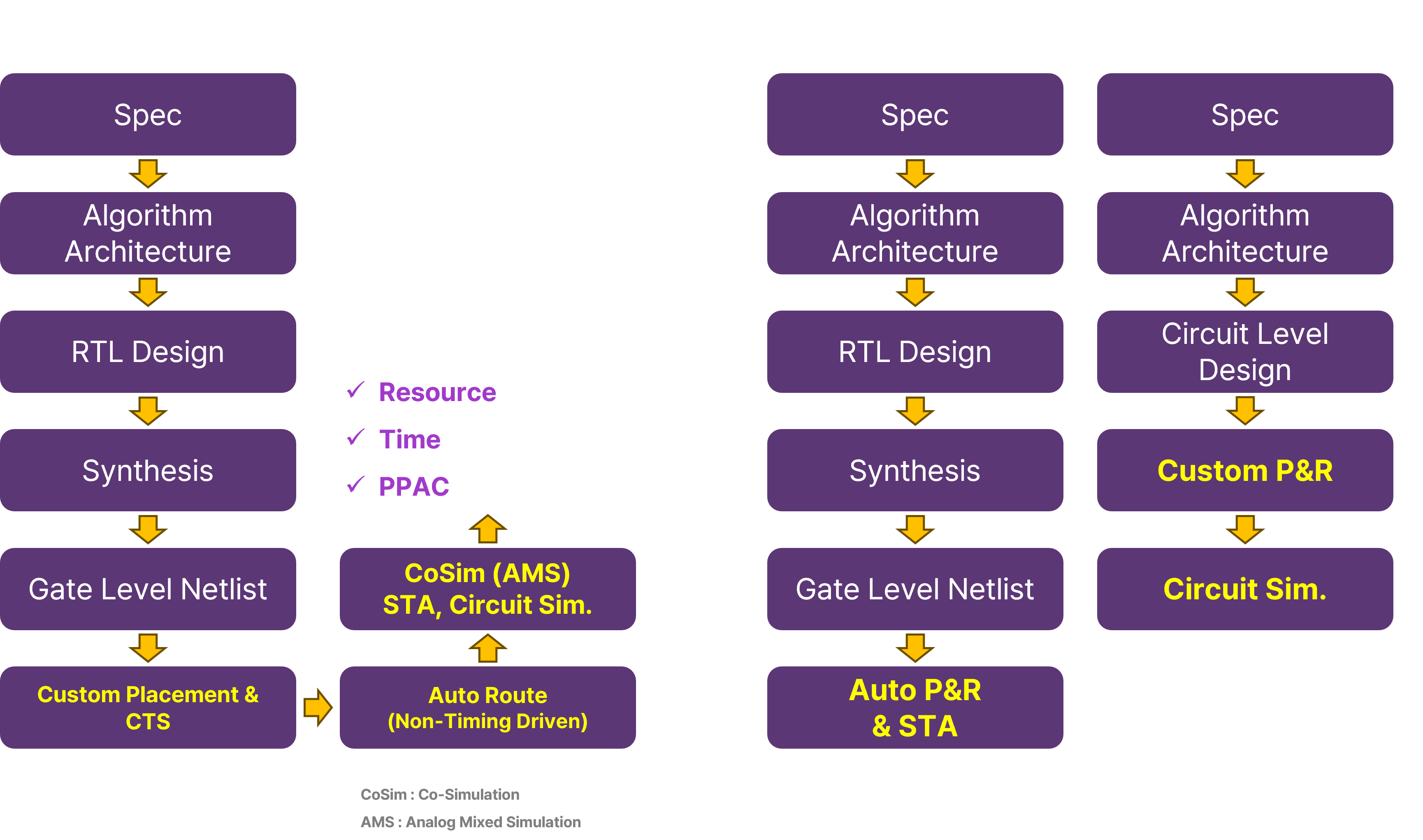
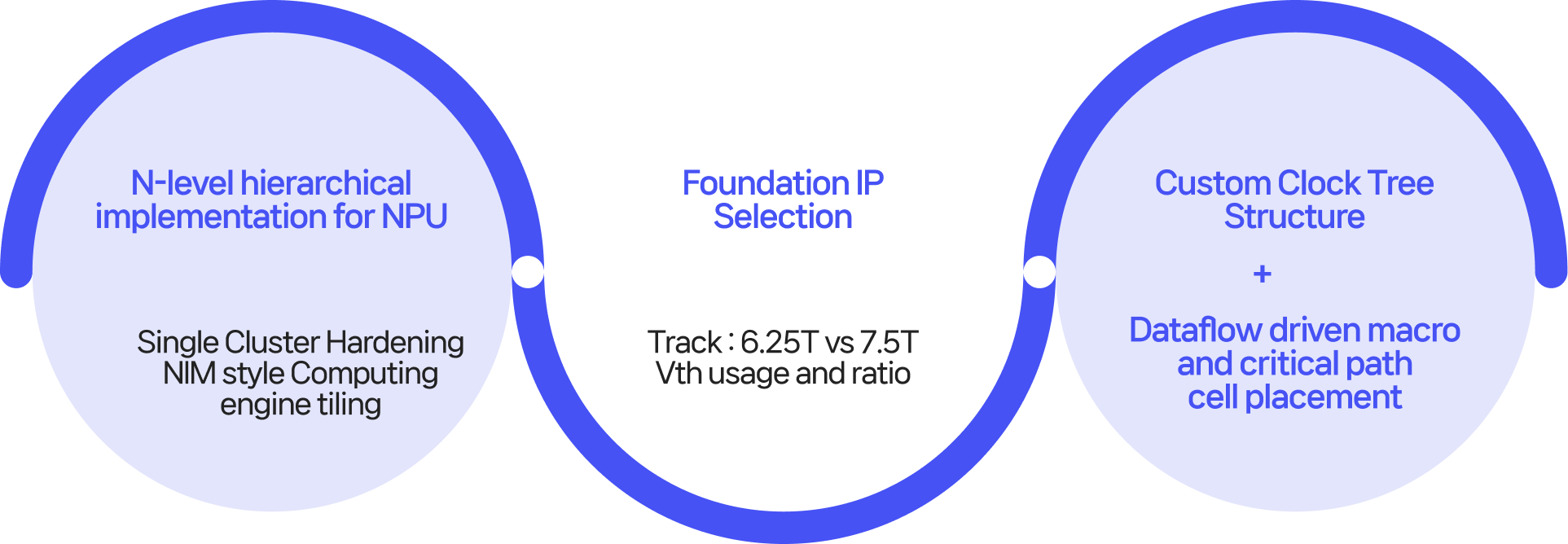
Logical/physical co-design

a. Grouping of tiling and hardening/basic processing elements (PEs) by application workload

b. Algorithm and gate-level optimization of critical operators ex) 4NM FinFET optimization Self-Shut-Off Pulsed Latches


c. PPAC(Power, Performance, Area, Cost) PE core enhancement and full chip layout for optimization

Optimized for customer operating environment

a. Dependable Performance Harvesting Technology – Patent Pending; Bad Core Management
b. Heat Dissipation Full Custom Layout

- 0.3V Library Re-Characterization and Near Threshold Computation

- Dependable Low Voltage IO Design supporting Fine-grained multi-power domain

- Undershoot / Overshoot Protection Circuit

- Revolutionizing Heat Transfer Design: Experience optimal thermal dissipation through our cutting-edge Hybrid P&R Layout technology, directly integrated into the ASIC for superior microchannel and heat sink performance. We guarantee the shortest heat dissipation path from the cells at the base to the RDL at the top, maximizing surface area contact with the cooling liquid for unparalleled thermal management.

- Experience Performance Beyond Limits: With the superior cooling efficiency of our immersion cooling systems, we empower higher operational frequencies without the risk of thermal throttling, pushing the boundaries of peak performance

- Soteria’s Advance Physical Implementation

Physical Implementation Engineer

Streamlined Logical-Physical Design Fusion:

Through meticulous tiling and hardening, we adapt to application workloads, ensuring optimal grouping of Primary Processing Elements (PE) for maximum efficiency and performance.

Enhancement of Vital Operators (Addressors, Multipliers, and more):

We achieve excellence through algorithmic and gate-level enhancements, such as advanced Dynamic, Domino Design, and asynchronous operation, to sharpen performance and deliver unprecedented results.

PE Core Strengthening and Comprehensive Chip Layout:

We strive for PPAC (Power, Performance, Area, Cost) optimization, reinforcing our Primary Processing Element (PE) cores and executing a full chip layout for maximum efficiency and cost-effectiveness.

Reliable Performance Harvesting Technology:

We focus on the management of Bad Cores and defective parts (ASIC Fault) to secure dependable performance. Our advanced technology effectively handles faults in ASICs, ensuring enhanced performance and stability.

Standard Cell based Full custom layout

  • Competitive TAT for post-layout timing analysis and timing closure
  • Ensure correct timing analysis at all design specific mode and corner combinations
  • In-house flow that makes full custom layout DB apply like Auto PnR DB
  • Configure physical hierarchy
  • Schematic vs physical cell binding
  • Update components and nets
  • Extract DEF and LEF2SPEF RC extraction

Signal & Power Integrity Engineer

Responsibilities and Opportunities

– Chip-level & Package-level SI/PI simulations.

– Collaborate with external SI/PI service providers

Key Qualifications

– Master’s degree or higher in EE

– Deep understanding of the theory of signal transmission and electromagnetic.

– Ability to work effectively in a production environment and deliver working solutions.

– Familiarity with IBIS AMI specification, model generation and simulation in commercial EDA tools such as Hspice and ADS.

Ideal Qualifications

– Experienced in designing HPC ASIC Accelerator Chip.

Physical Implementation Engineer

Responsibilities and Opportunities

– Implement the physical design (RTL2GDS, CDL2GDS) to achieve the best PPA.

– Support DSPs and/or contractors to do their best within the target TAT.

– Suggest architectural changes to improve the final QoR.

Key Qualifications

– Bachelor’s degree in Electrical Engineering or equivalent practical experience.

– 3 years of experience with EDA tool workflows in a semiconductor environment.

– Experience in scripting (e.g., Python, Tcl, Skill) for workflow automation and data visualization.

Ideal Qualifications

– Synthesis, STA, Simulation.

– Floorplan/Power planning, P&R, PV.

– CTS.

– V-XL/MXL P&R.

– Calibre LVS/DRC, StarRC.

– EM, PERC.

Global Marketing

Responsibilities and Opportunities

– Close external technology exchange with Samsung and DSP.

– Establishment of strategies and plans related to domestic semiconductor support projects.

– Visualize and document technology development reports.

– Understand market trends and proceed with internal reflection process.

– Responding to overseas customers and managing customers.

– Marketing Performance Indicators Management.

– General Import and export business.

Key Qualifications

– Semiconductor product marketing experience.

Ideal Qualifications

– Samsung (Foundry, SLSI, Memory) Marketing Experience.

SoC Engineer

Responsibilities and Opportunities

– Co-work closely with cross-functional teams for integrating SoC.

– Co-work and communicate with DSP for SoC implementation.

– Co-work for performing silicon bring-up and debug.

Key Qualifications

– Experience on multiple core CPU sub-system.

– Experience with various peripherals such as UART, SPI, I2C, I2S, GPIO and so on.

Ideal Qualifications

– Proficiency with industry-standard EDA tools relating to SoC integration.

Front-End Design (AI ASIC design)

Position Overview

We are looking for a talented engineer with a minimum of 8 years of experience to join our Front-End Design team. This role focuses on AI Accelerator ASIC and NPU architecture design and optimization. The ideal candidate will have a strong background in RTL design, verification, and a comprehensive understanding of AI/Machine Learning algorithms.

Key Responsibilities

– Design and implementation of front-end architectures, including DC and STA.

– RTL design and verification using Verilog and VHDL.

– FPGA prototype development for AI accelerators.

– Performance analysis and power efficiency optimization.

– Integrated design and optimization of software and hardware components.

– Chip architecture design and logic verification.

– Collaboration with cross-functional teams to ensure seamless integration of designs.

– In-depth analysis and enhancement of data center and cloud computing environments.

Skills and Qualifications

Educational Background

– Bachelor’s or Master’s degree in Electrical and Electronic Engineering, Semiconductor Engineering, or a related field.

Technical Expertise

– Proficient in RTL design and verification (Verilog, VHDL).

– Skilled in FPGA prototype development.

– Expertise in performance analysis and power efficiency optimization.

– Strong understanding of AI/Machine Learning algorithms.

– Knowledge of data center and cloud computing environments.

Tools Proficiency

– Verdi, VCS, DC, PrimeTime (STA, PTPX), Formality, Spyglass.

Preferred Qualifications

– Experience in integrated software and hardware design.

– Strong problem-solving skills and ability to work in a collaborative environment.

Location

– Soteria lab in Pangyo, Republic of Korea

Front-End Design Engineer (Near Data Process design)

Position Overview

We are looking for a talented engineer with a minimum of 8 years of experience to join our Front-End Design team. The focus of this role is on Near Data Processing architecture design and optimization. The ideal candidate should have expertise in RTL design, verification, and experience with memory interface and PCIe protocol architecture

Key Responsibilities

– Design and implementation of front-end architectures, including DC and STA.

– RTL design and verification using Verilog and VHDL.

– FPGA prototype development for Near Data Processing systems.

– Design and optimization of memory interface architecture.

– Architecture design and implementation of PCIe protocol.

– Chip architecture development and logic verification.

– Collaboration with cross-functional teams to ensure effective integration of designs.

Skills and Qualifications

Educational Background

– Bachelor’s or Master’s degree in Electrical and Electronic Engineering, Semiconductor Engineering, or a related field.

Technical Expertise

– Proficient in RTL design and verification (Verilog, VHDL).

– Skilled in FPGA prototype development.

– Expertise in memory interface architecture design and optimization.

– Strong understanding of PCIe protocol architecture design and implementation.

Tools Proficiency

– Verdi, VCS, DC, PrimeTime (STA, PTPX), Formality, Spyglass.

Preferred Qualifications

– Experience in integrated software and hardware design.

– Strong analytical skills and ability to work collaboratively within a team.

Location

– Soteria lab in Pangyo, Republic of Korea

Submit Applications to HR@SOTERIA-SYS.COM